Samsung Semiconductor India expands R&D footprint with a new state-of-the-art facility in Bengaluru
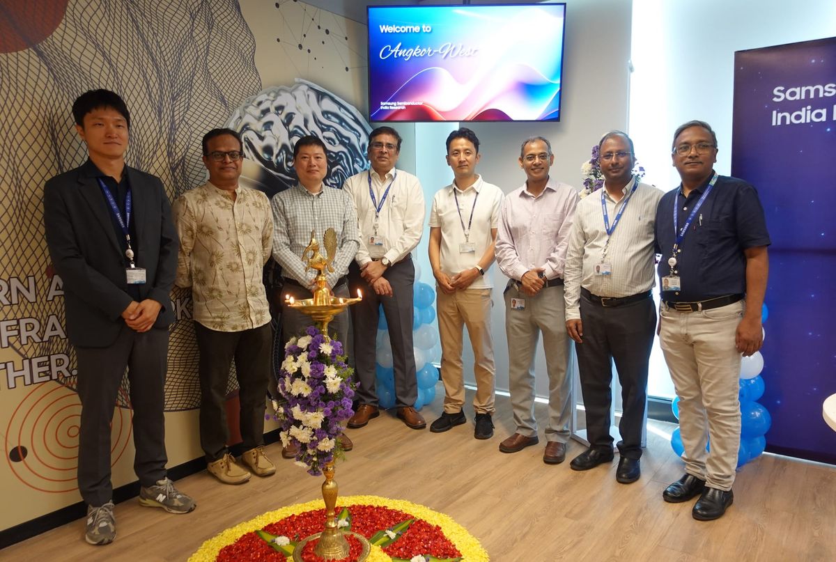
Samsung Semiconductor India Research (SSIR) announced the opening
of its new R&D facility in Bengaluru. The expansion marks a significant
milestone in SSIR's commitment to driving cutting-edge semiconductor research
and development in India while addressing the company's growing need for
advanced infrastructure. This is SSIR's second office in Bengaluru, with a
capacity to accommodate close to sixteen hundred professionals. Located at
Bagmane Capital Tech Park in Angkor-West, the facility spans 1, 60,000 square
feet across four floors.
The new campus of Samsung Semiconductor India Research (SSIR) features a modern, open-plan layout across four floors, encouraging collaboration and agility. The design includes designated hot-desking areas for workforce flexibility. There are over sixty (60) state-of-the-art meeting rooms for seamless communication, and amenities such as a fully equipped cafeteria, medical facilities, dedicated nap rooms, and recreational areas for rejuvenation for all employees. Additionally, transport shuttle services are also available which will further enhance convenience, ensuring a holistic work experience for SSIR employees.
"It is an exciting moment for us as the new facility in Bengaluru embodies our commitment to expanding our footprint in India and enabling a vibrant environment for our exceptional team members. This new hub reinforces SSIR's standing as a crucial player in Samsung Semiconductor’s global innovation ecosystem as we open the doors to new opportunities”, said Balajee Sowrirajan, EVP & MD at Samsung Semiconductor India Research.
SSIR currently has a strength of over four thousand five hundred (4500) employees and will add over seven hundred (700) people including fresh graduates as well as lateral hires across teams in India.